1. Background
With the continuous innovation in power electronics technology, switch-mode power supply (SMPS) technology has also been constantly evolving. Today, SMPS, known for its compactness, lightweight, and high efficiency, is widely applied in nearly all electronic devices. It stands as an indispensable power source amidst the rapid growth of the electronic information industry. However, EMC (Electromagnetic Compatibility) issues in SMPS remain a challenging concern.
2. Causes of Switch-Mode Power Supply Noise
What are the causes behind the generation of noise in switch-mode power supplies PCBA board?
(1) Instability in Voltage Output from Voltage Regulator Chips: The instability in the voltage output from voltage regulator chips may produce ripples. This instability could stem from errors in DC output terminals of the regulator chip or peak amplitude of power supply noise causing errors in the rising or falling edges of the switching frequency. The generation of ripples happens due to insufficient margin for power supply noise caused by the instability in the output of the voltage regulator chip.
(2) Inability of Voltage Regulators to Promptly Respond to Sudden Load Current Demands: Voltage regulators adjust their output current by sensing changes in the output voltage to regulate it back to the rated output value. Most commonly used voltage regulators adjust the voltage in milliseconds to microseconds. Therefore, when the frequency of transient load current changes exceeds the range between direct current or several hundred kHz, the voltage output of the regulator drops, leading to power supply noise.
(3) Voltage Drops in Power and Ground Impedances due to Transient Load Currents:
3. Measures to Suppress Switch-Mode Power Supply Noise
(1) Voltage Regulator Chip Selection: The first type of noise generated by switch-mode power supplies is inherent to the chip itself. Therefore, while accepting this noise is inevitable, opting for a better voltage regulator chip can reduce a portion of the noise, ensuring that the accepted noise level does not go too high.
(2) Parallel Connection of a Capacitor Before the Load:
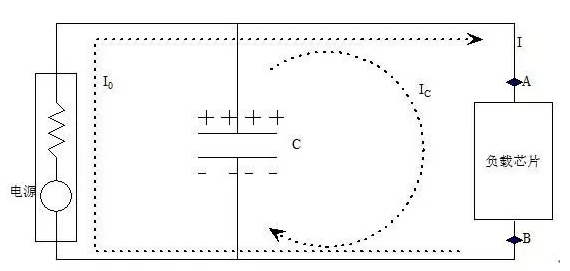
Figure 1: Decoupling Capacitor Circuit
When the load current remains constant, its current is supplied by the stable voltage source part, marked as I0 in Figure 1, as indicated. During this time, the voltage across the capacitor matches the load voltage, causing the current Ic to be zero, storing a significant amount of charge across the capacitor’s terminals.
When the load’s transient current changes, the voltage across the capacitor changes, leading to a flow of current Ic. As per the capacitor equation:
As long as the capacitance C is large enough, even with a small voltage change, the capacitor can provide a sufficient amount of current to meet the transient load current requirement. This ensures that the voltage variation at the load chip remains within an acceptable range. In essence, the capacitor stores a portion of electrical energy in advance and releases it when needed by the load, acting as an energy storage element.
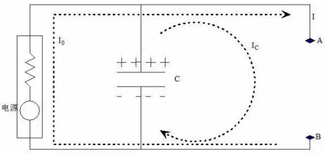
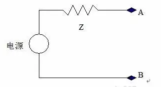
From another perspective, this capacitor functions as a power source. Viewed from points A to B in Figure 2, the power supply and capacitor can be equivalently replaced with a power supply system as shown in Figure 3.
Figure 2: Equivalent Circuit
Figure 3: Equivalent Circuit
The goal of this design is to keep the voltage variation between points A and B minimal, irrespective of how the load’s transient current changes, which implies that the impedance Z of the power system must be sufficiently low. In Figure 2, we achieve this requirement through a decoupling capacitor, thus reducing the impedance of the power supply system.
(3) Ensuring High-Quality Ground Plane on PCB Boards:
On a PCB board, any electrical path unavoidably possesses impedance, whether it’s a complete power plane or power leads. For multi-layered boards, a complete power plane and ground plane are usually provided. The output of the voltage regulator is first connected to the power plane, where the current flows through it to reach the load’s power pins. The path for the ground is similar to that of the power, except the current path becomes the ground plane. Hence, having a good, complete ground plane is extremely necessary.
4. Conclusion
Although switch-mode power supplies find extensive application, their EMI (Electromagnetic Interference) problems remain a primary concern. This article mainly analyzes three reasons behind switch-mode power supply noise generation and the corresponding measures. Subsequent articles will continue to delve into more topics related to power supply noise. Stay tuned for more updates.


