As a leading electronic manufacturing service provider, CEN excels in delivering high-quality PCB assemblies. One of the key processes ensuring this quality is Automated Optical Inspection (AOI). This article explores AOI’s vital role in PCB fabrication and assembly, leveraging our extensive experience to enhance understanding and SEO optimization.
What is Automated Optical Inspection (AOI)?
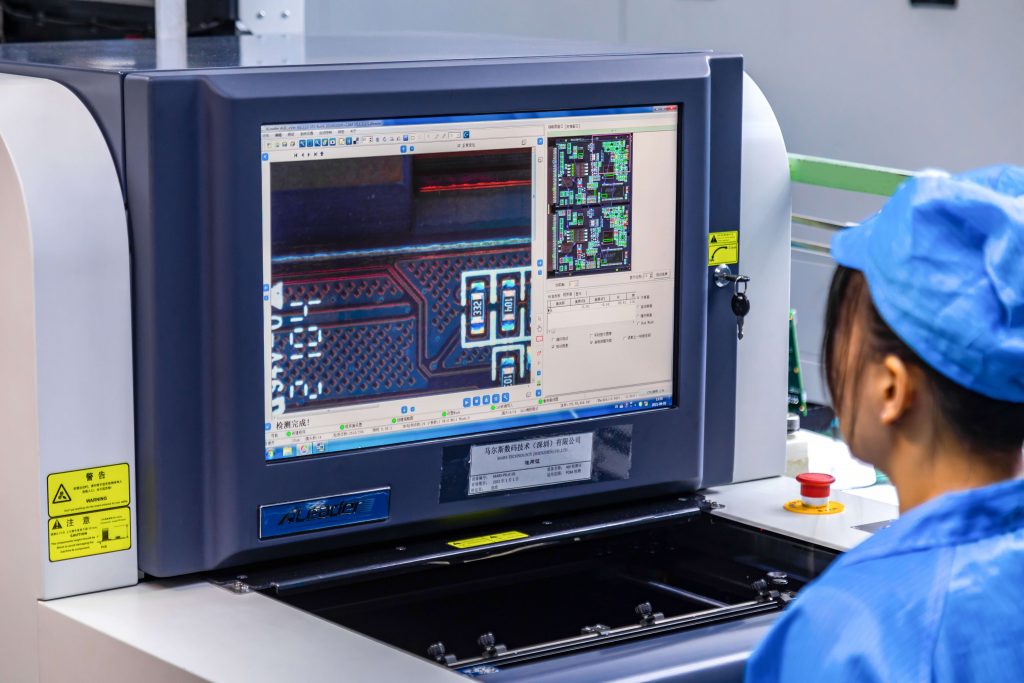
Automated Optical Inspection (AOI) is a sophisticated machine-based technique used to inspect printed circuit boards (PCBs) for defects. AOI is essential for identifying surface defects, dimensional inaccuracies, and component placement issues. As PCBs become more complex, manual inspection becomes impractical, making AOI indispensable for maintaining high quality and efficiency in PCB production.
How Does AOI Work?
AOI systems utilize high-resolution cameras and advanced image processing software to capture and analyze images of PCBs. The process involves comparing the captured images against a predefined set of standards or a “golden” board. Any deviations from these standards are flagged as potential defects. This method ensures thorough inspection, covering:
- Surface Defects: Scratches, nodules, and other surface anomalies.
- Dimensional Defects: Open circuits, short circuits, and improper solder thickness.
- Component Placement Defects: Misaligned, missing, or incorrect components.
Advantages of Automated Optical Inspection
- Positional Accuracy: AOI systems offer sub-pixel accuracy, crucial for detecting small positional deviations that could lead to defects, especially with miniaturized components.
- Cost-Effectiveness: By improving the pass rate of PCBs, AOI reduces overall production costs.
- Versatility: AOI is effective for both bare PCBs and assembled PCBs, inspecting for issues such as solder shorts, opens, insufficient solder, polarity, and component values.
- Programmable Lighting: Dynamic lighting arrays, customizable within the inspection software, enhance defect detection by adjusting lighting angles and colors to highlight various defects.
- Data Collection and Analysis: AOI systems collect and retrieve inspection data in various formats, aiding in quality control and process improvement.
- Flexibility: AOI can be integrated at any stage of the manufacturing process. However, it’s most effective after reflow soldering, where most defects typically occur.
Importance of AOI in PCB Production
Ensuring that PCBs are free from defects is crucial for their performance and reliability in electronic products. AOI plays a pivotal role in this by:
- Enhancing Quality Control: By detecting and correcting defects early in the production process, AOI helps maintain high standards of quality.
- Reducing Production Costs: Early defect detection prevents costly rework and scrap.
- Supporting High-Volume Production: AOI’s speed and accuracy make it ideal for inspecting large volumes of PCBs efficiently.
Common Defects Detected by AOI
For Surface-Mounted Technology (SMT) inspection, AOI can identify:
- Soldering Issues: Insufficient or excessive solder joints, solder bridging, tombstoning, and lifted leads.
- Component Issues: Incorrect, missing, skewed, or misplaced components, wrong polarity, and billboarding.
- Surface Defects: Scratches, nodules, and damaged components.
For bare PCB inspection, AOI detects:
- Circuit Issues: Short circuits, line width violations, and spacing violations.
- Component Mounting Issues: Missing pads, excess copper, and incorrect hole placement.
AOI Application Areas
AOI is critical in various stages of PCB manufacturing, including:
- Short Circuits: Detecting unintended connections between conductive paths.
- Line Width Violations: Ensuring traces are within specified width tolerances.
- Spacing Violations: Verifying adequate spacing between conductive elements.
- High-Frequency Applications: Ensuring signal integrity in high-frequency circuits.
- High-Power Loads: Checking PCBs designed to handle significant power loads for reliability.
Conclusion
Automated Optical Inspection (AOI) is an essential tool in PCB fabrication, ensuring the production of high-quality, reliable PCBs. At CEN, we are committed to adhering to the strictest manufacturing and assembly standards, utilizing AOI and X-Ray inspection to deliver superior products to our customers. AOI not only enhances quality but also reduces costs and improves overall production efficiency.
For more information on our PCB assembly services and how AOI can benefit your projects, contact us today.